04ELECTRONICS / PCB
SCHEMATIC → BOARD → HARDWAREHARDWARE ENGINEERING
ELECTRONICS / PCB
Turning system requirements into a board means separating power, sensing, processing and actuation clearly enough that the hardware can be routed, fabricated, assembled and debugged.
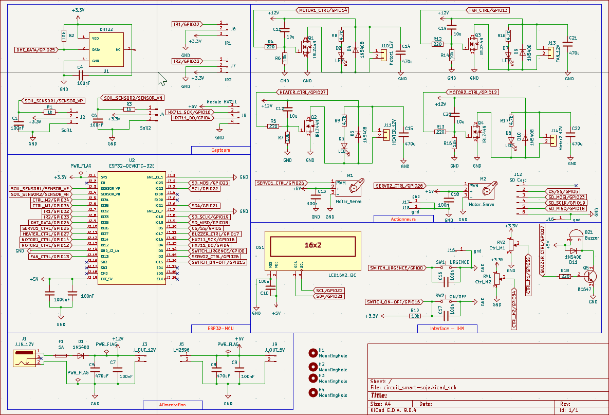
SCH / SYSTEM MAPFunctional segmentation before routing
LAYOUT / MANUFACTURING
From logical blocks to physical constraints.
Power paths, sensitive signals, connectors, protection components and mechanical clearances all become physical decisions during PCB layout. The deliverable is not the KiCad canvas — it is a board that can actually be fabricated and integrated.
KiCad schematic→PCB layout→3D check→Gerber / DFM
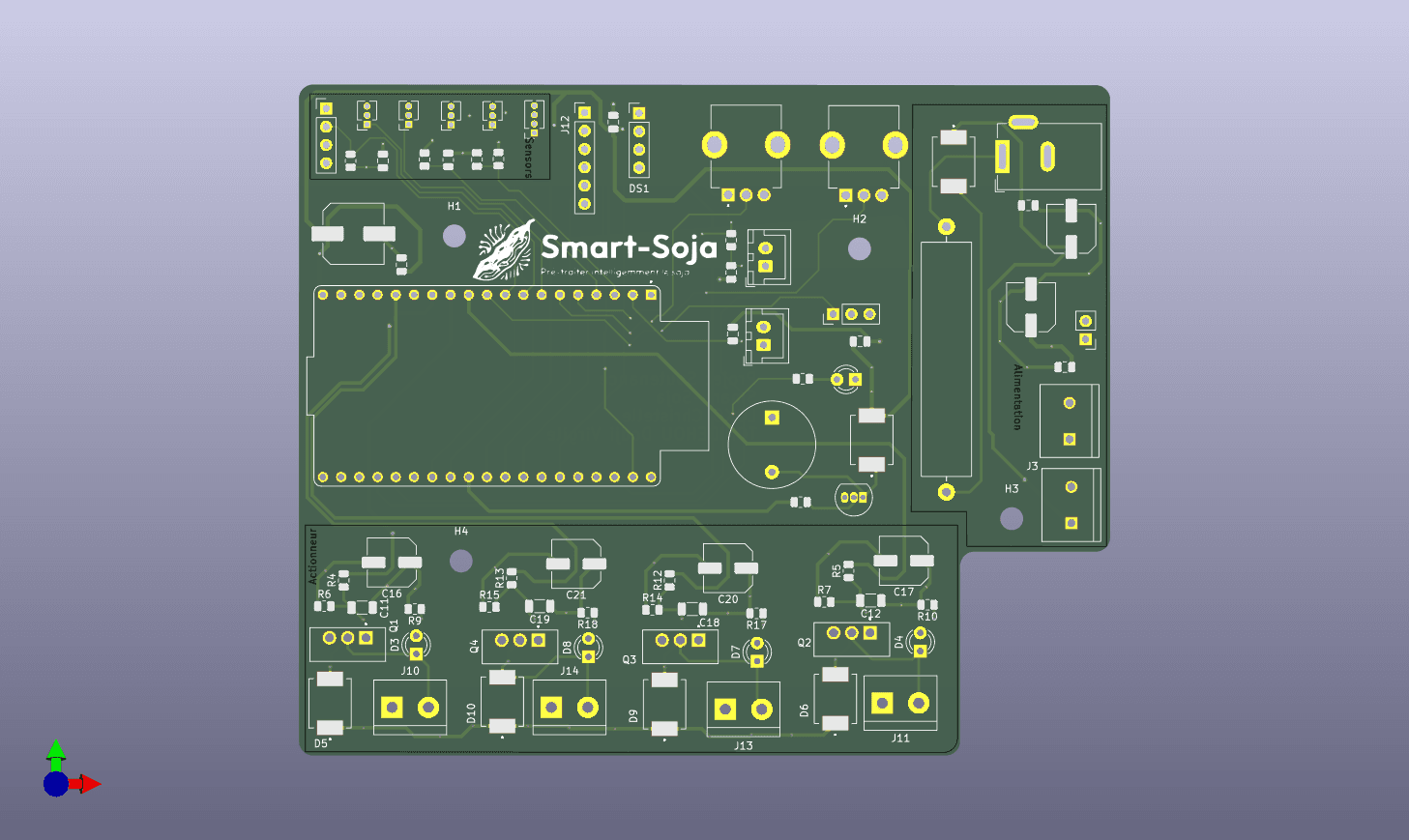
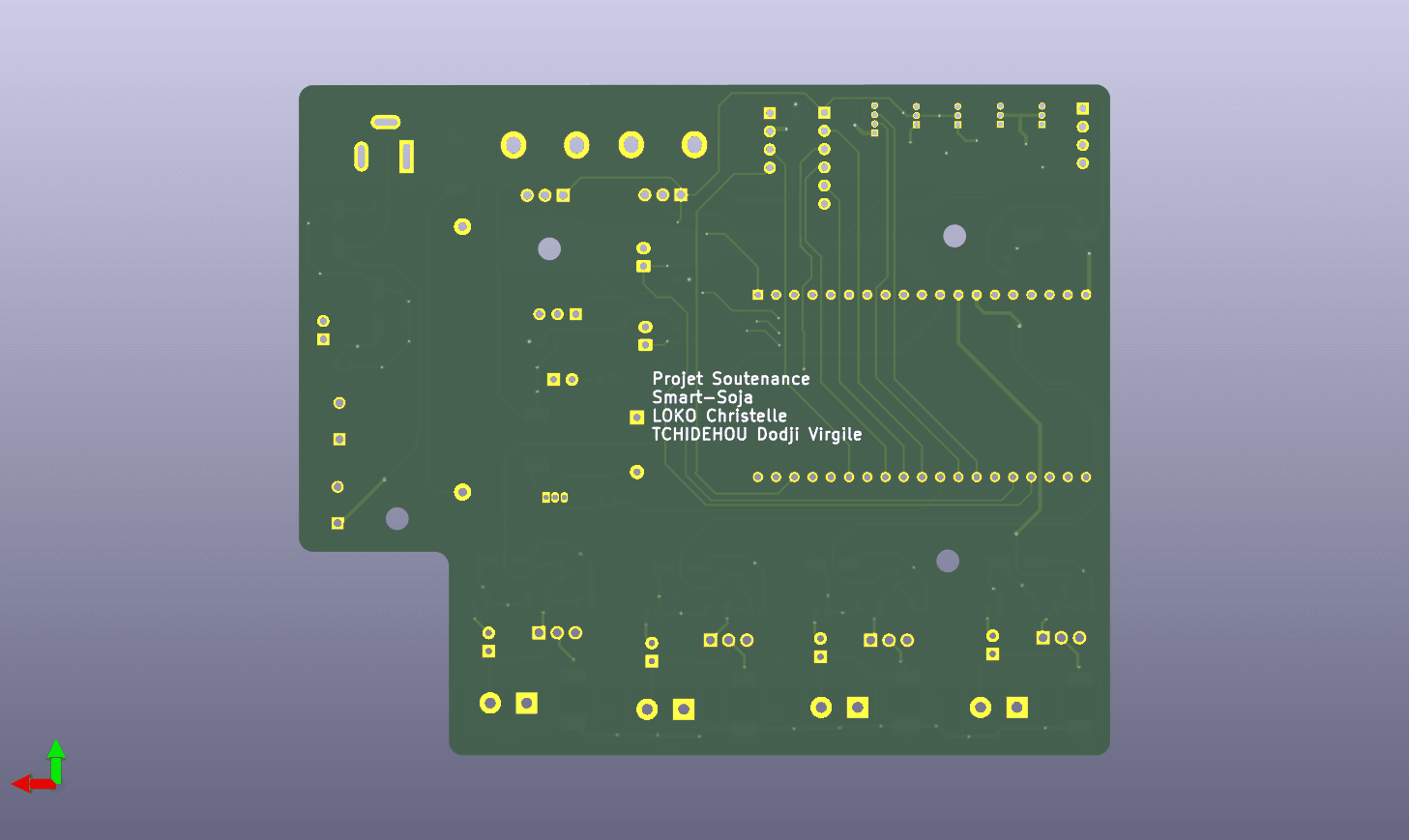
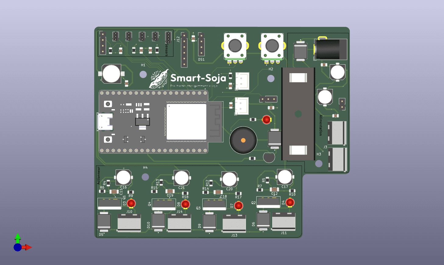 PCB / 3D CHECK
REALITY CHECK
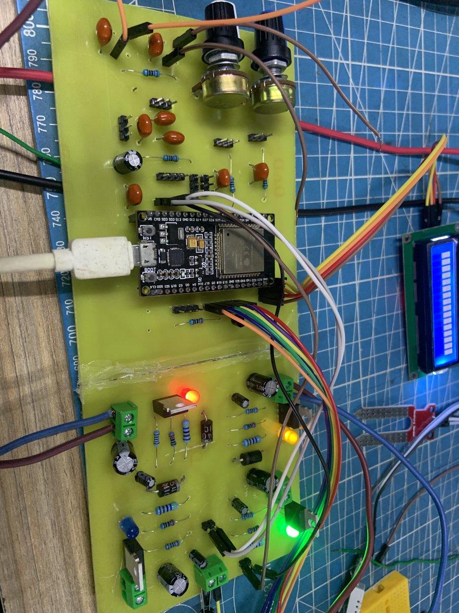
The board is only useful when the machine accepts it.
Connectors, wiring, serviceability, power handling and debugging matter just as much as the schematic. The electronics case closes only when the physical system can use it reliably.
Explore PCB sources ↗